This is
a circuit designed
to boost the output of a DDS signal generator or VFO to the level where
it could be a QRP transmitter or could be used to drive a boatanchor
type tube transmitter. I have several DDS units, including the
first NJQRP DDS and the DDS unit designed by Trevor Jacobs, K6ESE.
They typically output a signal of a few dBm (one to several
milliwatts) RF power after taking the DDS output through a single MMIC
amplifier stage.
It all started when a friend bought this huge Globe King 400 AM boatanchor transmitter, which doesn't have a VFO. After some discussion, I suggested a DDS with something to boost the output. (Actually, we never did try it with the Globe King.)
The circuit is a class-A BJT transistor stage with a power gain of about 26dB to get the output to around 200mw and then a MOSFET power amplifier, probably closer to class C than AB, to take that up to about 5 watts on 40 meters. The second stage is based on figure 2.98 of EMRFD with some changes made to the biasing.
Here are a couple of corrections (thanks WA0ITP): First, the RFC core isn't a FT37-43 because 9 turns would give a lot more than 5.2 uH. I used an unknown core, but my goal was to get a minimum reactance of 120 ohms on the lowest band (3.5 MHz) of interest. So do that. And, judging from the photo of the board, I used an IRF510A, not an IRF510. Note that I marked it on the device with a Sharpie.
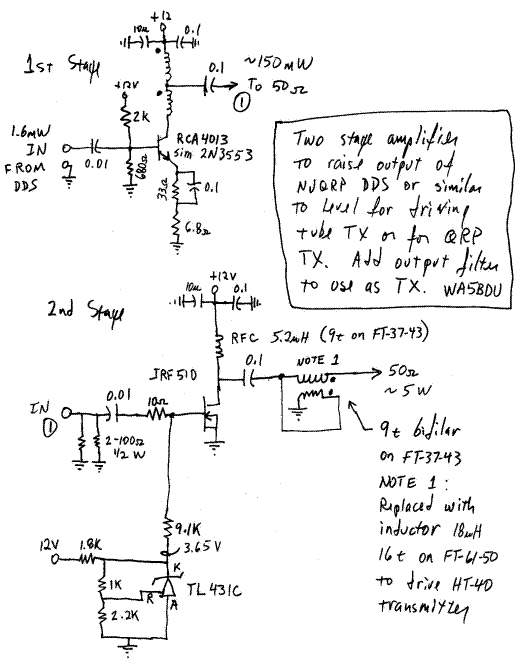

The
first stage is a class-A BJT broadband amplifier. Since it is
designed for 50 ohms output, you could use it with your DDS for a
QRP transmitter of a quarter watt or so output by itself.
It draws 55mA at idle and dissipates 600mW with no drive
(dissipation drops when the stage is driven). I used a heat sink
and a transistor probably capable of a watt or so. Note that the
input resistance of the stage isn't necessarily 50 ohms (about 150 ohms
on 40 meters), so maximum transfer from the DDS isn't achieved.
Not an issue, but I mention it for completeness.
The second stage uses an IRF510A MOSFET, as much because I hadn't tried one before as anything else. But they're cheap too. The circuit is based on one in EMRFD, but I played with the bias stage just for fun. The EMRFD version is biased for AB and could be used for SSB. If you adjust my bias upward some, this circuit could do the same if not over-driven. But I wanted to keep idling current low, so I biased the MOSFET to around the point where conduction begins. I actually did some tests on my particular MOSFET to come up with the value. I think I have 5 or 10 mA of idling current versus 100mA used for class AB. With my heat sink though, I'm sure I could run AB if I wished. By replacing the 1k and 2.2k resistors with a pot, you could adjust idling current easily.
The input has two resistors in parallel to provide the 50 ohm load. Thus most drive power is "wasted" there. But remember that the gate has a lot of capacitance to ground and in the interest of stability and waveform purity, this swamping is a good thing.
The output network in both stages is the familiar 4:1 transformer with bifilar winding, transforming the 50 ohm load up to 200 ohms for the first stage, and down to 12.5 ohms for the second stage. The number of turns isn't critical, but is chosen to allow enough inductance at the lowest band (80 meters). You may or may not want to add some turns for operation on 160. Try it.
Do be aware that my second stage doesn't have a harmonic filter. The reason is that I intended it to drive a transmitter where the driven stage is likely to be a frequency multiplier. So harmonic content could be desirable at that early stage. To use this stage as a transmitter, add a harmonic filter designed for 50 ohms input and output resistance.
Driving the HT-40 tube-type transmitter
I have an old Hallicrafters HT-40 novice transmitter. Before finding a suitable VFO, I experimented with driving it with my homebrew "Ugly Weekender" QRP transmitter. I determined that the HT-40's VFO input was high impedance, probably a few thousand ohms. So I figured I'd use a simple "L" network to transform it to 50 ohms. But while studying the HT-40's schematic, I saw that it already has a 22pF capacitor from grid to ground. That capacitor was one leg of the 'L', so all I needed was the inductor. Following that logic, I replaced the 4:1 output transformer with an 18uH inductor for this test. It worked OK. Grid current was at about half scale and I got full output from the HT-40.
There should be better ways of doing this that would give more flexibility. For instance, I have an EFHW (end-fed half wave) tuner that could probably match the unmodified 2nd stage to a couple thousand ohms at the tube TX's input.
One person asked why you need any power at all to drive the grid of a tube, since the impedance is essentially infinite. That's true, but I think if you drive into the region where the grid conducts and there is grid current over part of the cycle, you have to supply some real power.
Component selection and values
One fear I have when "publishing" something like this to the web is that readers might think every component value or choice is sacred and must be followed carefully, when a lot was just what I had in my junkbox, what was handy, and what might be fun to play with. And even things added that weren't really necessary.
I chose the RCA4013 transistor because I had several (unmarked) ones from Dan's in my junk box. It's alleged to be similar to a 2N3553. Use what you have if you think it can handle 600mW dissipation and the highest frequency you intend to use it on.
I have 10uF bypass capacitors on the +12 volt supply which are actually tantalums. There's a story here. I was trying in vain to drive my HT-40 on 6 meters (DDS at 8.348 MHz) but getting nowhere except some low frequency spurs. I think these extra caps were an attempt to deal with that issue. You probably don't need 'em.
I chose the IRF510 because as I said, lots of hams use 'em but I hadn't yet had the pleasure. And they're cheap. But they can be a problem when it comes to constant gain and/or power output across a wide range of frequency bands. I wasn't especially concerned with that so I went with the MOSFET.
The bias circuit is a story in itself. I used the TL431C 2.5 volt regulator because they're cheap and I have some in my junk box. Certainly don't special order this part. The zener method in EMRFD is fine, and even a simple resistive divider would be OK if your 12V supply is well regulated. For the 9.1k series resistor--a 10k would be OK.
Here we back out a little. The K6ESE DDS is at center and the HT-40 is at the rear. On the 2nd stage board, the 4:1 transformer is back in service and the output is being connected to a 40/30 meter LPF at front with two yellow toroids. At the left is an optical interrupter wheel I salvaged from a bathroom scale and interfaced to theDDS.
Some measurements
I hadn't made many measurements before deciding to document the amplifier on this web page. Measurements were made with the output configured for 50 ohms with the 4:1 transformer installed. First, I measured power output to a 50 ohm dummy load on 7.04 MHz. It was 5 watts and clipped on peaks viewed with my scope as expected. Next I installed a low-pass filter suitable for 40 and 30 meters and checked again. The power on 40 meters increased to 5.6 watts, which was a surprise to me. On 10.1 MHz, output dropped all the way to 1.9 watts. The waveform looked good on both bands. I also checked it on 80 meters although I didn't have a proper filter for that band. Battery voltage was 11.8VDC under load.
Full amp:
Next, I disconnected stage 1 and made some measurements on it alone, to validate that the drop in output with increasing frequency is due to the MOSFET stage. I found output pretty flat up to about 15 meters. After that, per my notes, the DDS's output also drops, so there's a compounding of effects.
Stage 1 Amp:
I haven't made a QSO with it yet. Where will I key it? Probably the 12V power to one or both stages. But I also need a way to make the DDS either inhibit its output or move off frequency when I'm in the receive mode, so it doesn't QRM me. The K6ESE board does have a T/R line I could use for a frequency shift.
Nick, WA5BDU
12/28/2007
The second stage uses an IRF510A MOSFET, as much because I hadn't tried one before as anything else. But they're cheap too. The circuit is based on one in EMRFD, but I played with the bias stage just for fun. The EMRFD version is biased for AB and could be used for SSB. If you adjust my bias upward some, this circuit could do the same if not over-driven. But I wanted to keep idling current low, so I biased the MOSFET to around the point where conduction begins. I actually did some tests on my particular MOSFET to come up with the value. I think I have 5 or 10 mA of idling current versus 100mA used for class AB. With my heat sink though, I'm sure I could run AB if I wished. By replacing the 1k and 2.2k resistors with a pot, you could adjust idling current easily.
The input has two resistors in parallel to provide the 50 ohm load. Thus most drive power is "wasted" there. But remember that the gate has a lot of capacitance to ground and in the interest of stability and waveform purity, this swamping is a good thing.
The output network in both stages is the familiar 4:1 transformer with bifilar winding, transforming the 50 ohm load up to 200 ohms for the first stage, and down to 12.5 ohms for the second stage. The number of turns isn't critical, but is chosen to allow enough inductance at the lowest band (80 meters). You may or may not want to add some turns for operation on 160. Try it.
Do be aware that my second stage doesn't have a harmonic filter. The reason is that I intended it to drive a transmitter where the driven stage is likely to be a frequency multiplier. So harmonic content could be desirable at that early stage. To use this stage as a transmitter, add a harmonic filter designed for 50 ohms input and output resistance.
Driving the HT-40 tube-type transmitter
I have an old Hallicrafters HT-40 novice transmitter. Before finding a suitable VFO, I experimented with driving it with my homebrew "Ugly Weekender" QRP transmitter. I determined that the HT-40's VFO input was high impedance, probably a few thousand ohms. So I figured I'd use a simple "L" network to transform it to 50 ohms. But while studying the HT-40's schematic, I saw that it already has a 22pF capacitor from grid to ground. That capacitor was one leg of the 'L', so all I needed was the inductor. Following that logic, I replaced the 4:1 output transformer with an 18uH inductor for this test. It worked OK. Grid current was at about half scale and I got full output from the HT-40.
There should be better ways of doing this that would give more flexibility. For instance, I have an EFHW (end-fed half wave) tuner that could probably match the unmodified 2nd stage to a couple thousand ohms at the tube TX's input.
One person asked why you need any power at all to drive the grid of a tube, since the impedance is essentially infinite. That's true, but I think if you drive into the region where the grid conducts and there is grid current over part of the cycle, you have to supply some real power.
Component selection and values
One fear I have when "publishing" something like this to the web is that readers might think every component value or choice is sacred and must be followed carefully, when a lot was just what I had in my junkbox, what was handy, and what might be fun to play with. And even things added that weren't really necessary.
I chose the RCA4013 transistor because I had several (unmarked) ones from Dan's in my junk box. It's alleged to be similar to a 2N3553. Use what you have if you think it can handle 600mW dissipation and the highest frequency you intend to use it on.
I have 10uF bypass capacitors on the +12 volt supply which are actually tantalums. There's a story here. I was trying in vain to drive my HT-40 on 6 meters (DDS at 8.348 MHz) but getting nowhere except some low frequency spurs. I think these extra caps were an attempt to deal with that issue. You probably don't need 'em.
I chose the IRF510 because as I said, lots of hams use 'em but I hadn't yet had the pleasure. And they're cheap. But they can be a problem when it comes to constant gain and/or power output across a wide range of frequency bands. I wasn't especially concerned with that so I went with the MOSFET.
The bias circuit is a story in itself. I used the TL431C 2.5 volt regulator because they're cheap and I have some in my junk box. Certainly don't special order this part. The zener method in EMRFD is fine, and even a simple resistive divider would be OK if your 12V supply is well regulated. For the 9.1k series resistor--a 10k would be OK.

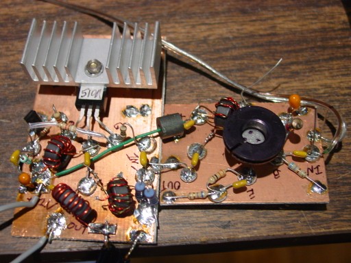
Here's
a photo of the board(s). The 1st stage is at the right, the
transistor wears a heat sink hat and the 4:1 transformer is above left
of it. The ferrite bead in the 12VDC jumper between the boards isn't
shown on the schematic and probably unnecessary. The IRF510A's
heat sink sits on stand-offs made of two grommets. At the bottom
right is the disconnected 4:1 transformer and left of it is the
substituted 18uH inductor used to interface with the HT-40. The
two blue resistors right of the 4:1 xfmr are the two 100 ohm input
resistors. At the left edge down from the heat sink is a black
plastic T092 device which is the TL431C regulator.
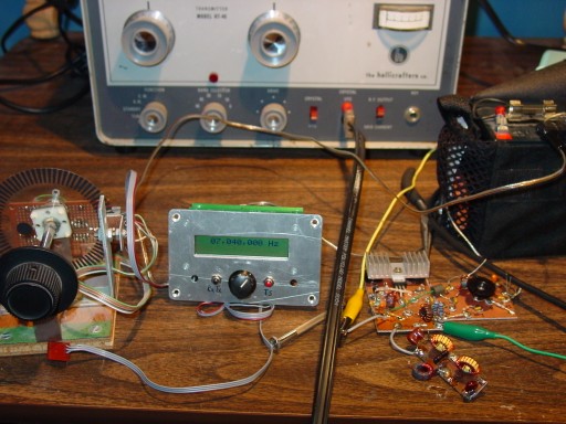

Here we back out a little. The K6ESE DDS is at center and the HT-40 is at the rear. On the 2nd stage board, the 4:1 transformer is back in service and the output is being connected to a 40/30 meter LPF at front with two yellow toroids. At the left is an optical interrupter wheel I salvaged from a bathroom scale and interfaced to theDDS.
Some measurements
I hadn't made many measurements before deciding to document the amplifier on this web page. Measurements were made with the output configured for 50 ohms with the 4:1 transformer installed. First, I measured power output to a 50 ohm dummy load on 7.04 MHz. It was 5 watts and clipped on peaks viewed with my scope as expected. Next I installed a low-pass filter suitable for 40 and 30 meters and checked again. The power on 40 meters increased to 5.6 watts, which was a surprise to me. On 10.1 MHz, output dropped all the way to 1.9 watts. The waveform looked good on both bands. I also checked it on 80 meters although I didn't have a proper filter for that band. Battery voltage was 11.8VDC under load.
Full amp:
40M, no filter: 5.6
watts
40M, filter: 5.0 watts
30M, filter: 1.9 watts
80M (note): 10 watts (note: filter cut-off too high for 80 so some waveform distortion was seen here)
The strong variation with frequency is
probably due to the high input capacitance (130pF) of the MOSFET gate.
The response could be flattened with some effort, but that's
beyond the intended scope of this project.40M, filter: 5.0 watts
30M, filter: 1.9 watts
80M (note): 10 watts (note: filter cut-off too high for 80 so some waveform distortion was seen here)
Next, I disconnected stage 1 and made some measurements on it alone, to validate that the drop in output with increasing frequency is due to the MOSFET stage. I found output pretty flat up to about 15 meters. After that, per my notes, the DDS's output also drops, so there's a compounding of effects.
Stage 1 Amp:
3.60 MHz: 250mw
7.04 MHz: 250mw
10.1 MHz: 260mw
14.06MHz: 280mw
18.07MHz: 260mw
21.1 MHz: 240mw
24.4 MHz: 180mw
28.3 MHz 160mw
Next?7.04 MHz: 250mw
10.1 MHz: 260mw
14.06MHz: 280mw
18.07MHz: 260mw
21.1 MHz: 240mw
24.4 MHz: 180mw
28.3 MHz 160mw
I haven't made a QSO with it yet. Where will I key it? Probably the 12V power to one or both stages. But I also need a way to make the DDS either inhibit its output or move off frequency when I'm in the receive mode, so it doesn't QRM me. The K6ESE board does have a T/R line I could use for a frequency shift.
Nick, WA5BDU
12/28/2007